


The fine details of surface roughness
To contact or not to contact
In the world of quality control within metalworking manufacturing, the measurement of surface finish is a complex subject with multiple standards for defining the various elements of roughness, waviness and other parameters required for the description of machined surfaces.
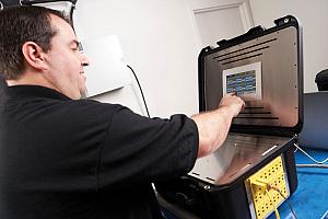
For decades the use of diamond-tipped contact profilometers have been the standard tools used to measure surface finish qualities, but as optical technologies have evolved the introduction of more detailed surface topography images are being made available for extremely demanding applications where surface finish readings are critical.
The typical contact surface measurement instruments come in a variety of shapes and sizes, including handheld portable devices and dedicated bench type machines, and because of their relative affordability and ease of use, these instruments continue to be the most common tools used for surface metrology. Peter Detmers, vice president sales with Mitutoyo Canada, has been involved with doing surface roughness measurements for some 25 years. He relates a long-term standard used for measuring the roughness average (Ra) of a component would involve using a stylus-type profile measuring device and measuring a 0.8 mm cut-off five times, and depending on which parameter you’re using, the Ra number is generated from those five different sections.
Unlike the stylus on a turntable which follows a groove and converts vibrations into sound, the stylus on a profilometer moves in a linear path and moves up and down over the surface and the device calculates surface roughness or other topographical data from the variations.
“Most of the standards in the industry were written around the contact-type technology, a 2D reading,” says Detmers.
Surface finish has an effect on many different aspects of a part’s functionally. Detmers suggests that most shops in automotive, aerospace and even general machining will have at least one if not many portable profilometers on the floor as well as dedicated bench-top units.
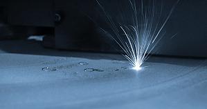
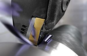
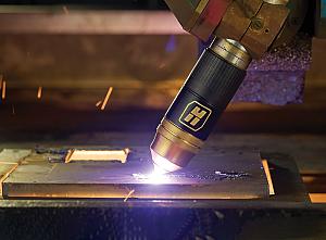
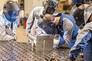
[gallery type="slideshow" link="none" ids="108706,108705,108703,108704,97664"]
These surface measuring tools are used to read surface finish on external surfaces and internal surfaces, including small bore holes.
And manufacturers of stylus instruments have made tips very small to get into those types of surfaces.
A cylinder bore is a common example used for the importance of surface finish. If a piston and the bore contact each other eventually they’re going to weld together, so the bore must be able retain oil to keep a viscous layer between the cylinder and the bore.
In measuring the bore, the desired surface would have low peaks and deep valleys to hold the oil.
The most recent developments in stylus-based measurement has included the integration of surface finish probes into common CMM (coordinate measuring machines). Renishaw has the REVO SFP1 probe, a tip-sensing probe for use on its REVO measuring head and probe system. Mitutoyo also has its SURFTEST probe which can be fit on the rotary head of the Renishaw PH10 system on Mitutoyo’s CMM systems. And the Zeiss ROTOS is a roughness sensor that can be incorporated on a Zeiss production CMM. All of these solutions eliminate having to reposition a workpiece on multiple devices and allow one machine to compile all measurement data into one report.
One challenge may be justifying tying up an expensive CMM system when a less expensive surface measurement tool could be used for this process.
Beyond the stylus, non-contact optical solutions using light to measure the surface of components are capable of capturing more finite detail than the stylus tools, and perform the task much faster.
The data points compiled by optical devices are stitched together to form a point cloud which is digitally transformed into a 3D topographic image.
According to Rob Johnson, product manager for Carl Zeiss products, with Elliott Matsuura Canada, one area of strong market demand for detailed surface finish accuracy is within the automotive powertrain sector.
White light interferometry is one well established technology, proven to be very repeatable with a high degree of resolution, making it suitable as an optical profilometer.
Another is the confocal microscope.
Novacam Technologies of Point Claire, Quebec, manufactures fiber-based optical non-contact 3D profilometers using low coherence interferometry. Novacam’s profilometers allow for high-speed scanning and create surface maps providing detailed roughness data.
Novacom has created many small fiber-based probes that can be fed into small diameter bores or challenging environments, allowing the measurement of both dimension and roughness. Along with the many advantages of the optical solutions come higher costs admits Vuk Bartulovic, president of Novacam Technologies.
He says the technology is being applied in the auto industry today, for high-precision machined parts. “They are producing a lot of parts and the takt time is quite short, so in many cases you have only seconds to do the measurement,” he says, pointing to the benefit of speed with the optical solution.
Bartulovic also notes that recent requirements from aerospace and automotive call for finer resolutions. Already Novacam’s optical solutions can deliver sub-micron resolution (0.8 micron), and he suggests that the next generation instruments will go even further.
Another high resolution alternative is the confocal laser scanning microscope (CLSM) like the Olympus LEXT OLS4100 which has been optimized for surface imaging, optical profilometry and surface roughness measurement.
According to David Rideout, director of sales and marketing, industrial microscopes with Olympus, the laser is a very small spot size, and confocal removes all out-of-focus light capturing only high-resolution data and then compiles it into one 3D image.
“We’ve sold this solution into the aerospace industry, automotive, semiconductor, and archeology. For any industry that’s looking at surfaces at a sub-micron level it’s an appropriate instrument,” says Rideout.
For the industrial market, Olympus released its 4000 model with the ability to filter the data back down to replicate using a regular stylus-tipped contact profilometer.
“Profilometers have been around for a long time, so there’s a well-established comfort level there. When you want someone to try new technology you have to make them comfortable with that new technology,” says Rideout. “One way to do that is to give them what they’re used to as you take them to this new level of measurement.”
With the advancements of non-contact optical technology in the field of surface finish, the ISO 25178 standard has been developed for 3D surface metrology.
When comparing an interferometer with confocal, the interferometer offers a better depth of field for reading peaks and valleys, but the confocal is stronger in the xy and at reading angles, says Rideout.
He admits the laser confocal process is used more in a controlled environment and is more of an analysis tool and not used much in production.
For most metalworking machining applications the fine detail of the optical toolsare overkill, and because of the large cost differential between stylus instruments and optical, only if an application demands a non-contact solution would manufacturers select that option.
“Part of the reason is cost, another part is, where do you put this machine?” asks Detmers of Mitutoyo, who does offer optical solutions as well as tradition contact profilometers. He explains that because there are optics involved, vibrations can affect the measurement, and if you require a very high resolution measuring capability, you’ll need a suitable environment.
“In the metalworking industry, typically the only time somebody will ever bring up the idea of non-contact is if the scratch left behind by the diamond dragging across the part will affect the use of that part,” he says.
About the Author
About the Publication

subscribe now

Keep up to date with the latest news, events, and technology for all things metal from our pair of monthly magazines written specifically for Canadian manufacturers!
Start Your Free Subscription- Stay connected from anywhere

Easily access valuable industry resources now with full access to the digital edition of Canadian Metalworking.

Easily access valuable industry resources now with full access to the digital edition of Canadian Fabricating & Welding.
- Trending Articles
1
Automating additive manufacturing

2
Sustainability Analyzer Tool helps users measure and reduce carbon footprint

3
CTMA launches another round of Career-Ready program

4
Sandvik Coromant hosts workforce development event empowering young women in manufacturing

5
GF Machining Solutions names managing director and head of market region North and Central Americas